
Component Orientation & Alignment
Figure No. 4-12 within J-Std-002 & the corresponding Figure 4 within BS EN 60060-2-69 (see diagram below) illustrates, in general, the correct orientation for different styles of components.
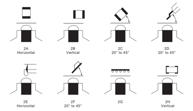
Illustrations 2A, 2B & 2C, depict the testing of chip style components. 2A being the optimum way for larger chip style components as the maximum area of the solderable surface is immersed in the solder, it also helps with getting the correct alignment.
However, when testing smaller chip style components 0603 or 0402 etc it is best to adopt the configuration shown in diagram 2B. This is because the area that the solder can wet onto is far larger i.e. the vertical face.
Illustration 2D depicts a “gull wing” leaded component such as a QFP or SOIC.
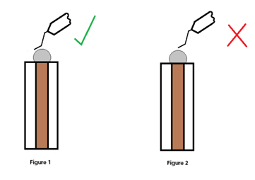
It illustrates how the toe of the lead will come into contact with the solder during the test - see Figure 2 below. This not the best practice as it will restrict the transfer of heat from the solder to the component that may generate a “false” failed test result. A better way to approach this is to set up the component alignment such that all the sole of the lead will come into contact with the solder – see Figure 1 below. This will ensure maximum heat transfer is achieved and in turn, will generate a more accurate test result.
Odd-Form Components
These type of components are generally large & bulky with a considerable thermal mass. If testing as a whole, it may require the solder temperature to be increased to 275°C or even hotter!!Test time should be increased to 10secs/20secs/30secs to overcome the thermal mass. Alternatively, if the component terminal can be removed and tested separately, the thermal mass problem will be eliminated.
Printed Circuit Boards
The testing of PCB pads generates many problems.
When selecting a PCB pad a large one is preferrable as this offers more solderable surface for wetting to occur and also provides the ability to use a larger globule i.e. 4mm.
Prepare the test sample as 10mm square as a minimum. This allows better support when fitting to the test clip.
Also, it’s best to have the solderable surface right up to the edge of the sample. This ensures that only the pad is in contact with the hot solder during the test.
Alignment of the PCB pad to the solder on the Globule is critical.
It’s necessary for the pad to touch the solder not on the top but using the curved section of the solder pellet similar to Figure 1 above. This allows better heat transfer from the solder to the pad. It’s important not to immerse too much of the pad into the solder because there needs to be a section of the pad available to accept the solder as it wets.
Another issue is thermal demand, because there could be a considerable amount of copper attached to the pad you are testing so the thermal demand could be high. Again, increasing the solder temperature & the test duration time should eliminate the thermal mass issue.
Ball Grid Arrays (BGAs)
The testing of a balled BGA is not at all practical. In essence, this comprises the presentation of molten solder (globule) to an existing ball of solder (BGA). Consequently, there is no contact with a solderable surface i.e the BGA pad, so any results obtained are quite meaningless.
Solderability testing is used to indicate the ability of a surface to be wet by molten solder.
The reason we do this is that the surface finish on components is not stable and deteriorates over time.
There are two types of generic solderable finishes, these are fusible and non-fusible. A fusible coating will melt or dissolve readily allowing a solder wetting front to spread across the termination. A non-fusible finish is typically a noble metal, such as silver or gold, and will only have an added layer produced by oxidation. In this context oxidation can form an oxide, but this can also be a sulphur, chloride, or any other oxidising molecule, that forms a surface compound.
Non-fusible coatings are expensive, and hence they tend to be thin. If thick, solderability can be retained indefinitely. A weakness of noble metal finishes is they can be applied too thinly or other complicating factors such as nickel corrosion on electroless nickel and gold immersion (ENIG) finishes, “black pad” can occur.
Fusible coatings are usually pure tin these days, although in the past would have been alloyed with lead. The oxidation issue is not a problem under normal conditions, because as the plating liquifies the oxide is broken up & is dispersed to the liquid/solid interface and so does not impede soldering. The ageing mechanism of concern is that of intermetallic (IMC) growth. Depending on time, temperature and quality the IMC can grow to the extent that it consumes all the plating, or as a minimum interferes with the spread of solder across the surface. The IMC growth is highly irregular, it does not grow as a planar surface.
So, what is the issue of solderability with BGAs? It is difficult to envisage either mechanism, oxidation or IMC growth effecting a BGA ball. The ball size is massive in the context of IMC growth, so IMC is not an issue. Since nearly all BGA balls are fusible, any oxidation will have no effect on the soldering process. Only non-fusible BGA balls or BGAs that have been stored in exceptionally harsh conditions, (not typical of storage) can be a reason to suspect the solderability of a BGA.